Class A , Class B And Class AB Amplifiers Full Details
Introduction
Class A Amplifiers offer a very
good linearity of the output, meaning that the signal is faithfully reproduced,
however their efficiency is very low, around 20-30 % in most of the cases. On
the other hand, Class B Amplifiers present a very high efficiency up
to 78.5 % but cannot reproduce the output faithfully. Indeed,
a crossover distortion appears in a push-pull configuration and the use of a
negative feedback is required to limit this effect.
In order to combine both the
excellent linearity of class A and the high efficiency of class B, the class
AB has been developed. In the very first section, we will present the
general functioning and characteristics of class AB amplifiers.
Thereafter, we will discuss the efficiency of class AB configurations. The
following section will present some possible biasing methods and we will
highlight that the diode biasing is the most appropriate. Finally we will see
that even the diode biasing method needs to be improved in order for the class
AB configuration to correctly amplify the signal with no crossover distortion.
Presentation of the Class AB
amplification
As the name refers to, class AB is
working half way between class A and class B amplifiers. The Figure
1 below shows the operating zone of class AB amplifiers in a (Vout,Iout)
characteristic graph.

fig 1 : Operating zone
of class AB amplifiers
Class AB amplifiers
can be biased by choosing an operating point along this blue line, excluding
the class A and class B biasing points. The choice of its location depends on
the desired levels of efficiency and linearity. If the class AB operating point
is closer to the class A operating point (resp. class B) than the class B
operating point (resp. class A) the circuit will behave more such as a class A
amplifier (resp. class B) by presenting a higher linearity but a lower
efficiency (resp. higher efficiency but lower linearity).
The conduction angle of class AB
amplifiers is therefore in the ]180°,360°[ range. This type of amplifier
conducts the signal more than 50 % of the time but less than 100 % such as
shown in the Figure 2 below :

fig 2 : NPN and
PNP-based class AB amplifier conduction angle
Both NPN and PNP-based class
AB behaviours are presented since a push-pull configuration is necessary, such
as for the class B amplifier, to combine the positive and negative half-waves
in order to reproduce the complete signal.
We can note that a small portion
of the signal is conducted simultaneously by the NPN and the PNP transistors.
This ensures that no crossover distortion is observed during the amplification
performed by class AB amplifiers.
Class AB efficiency
The formula of the efficiency (η)
for class AB amplifiers is similar to the class B configuration and is given by
the following equation :
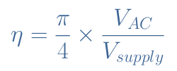
eq 1 : Efficiency of a push-pull class AB configuration
Where VAC represents
the AC fluctuation of the output signal. The maximum efficiency here, not only
depends on the maximized value of VAC, but also on the position
of the operating point along the operating zone (see Figure 1) :
- If the class AB amplifier is biased at the limit of
the cutoff point, VAC,max=Vsupply and
thus ηmax=π/4=78.5 %.
- If the class AB amplifier is biased at the limit of
the class A operating point, VAC,max=Vsupply/2 and
thus ηmax=π/8=39.3 %.
- In the other cases, the maximum efficiency of a class
AB amplifier will be in the ]39.3 % ; 78.5 %[ range.
Biasing methods
There are many ways of biasing
a class AB amplifier in order to create an interval of voltage
where the complementary transistors conduct simultaneously. In this section, we
will briefly present some of the possible biasing methods by highlighting their
advantages and disadvantages. The methods will be sorted by how relevant they
are, we will indeed begin by the most inappropriate to end with the most
common, easier to implement and efficient.
Voltage biasing
A very easy and intuitive method
is to bias directly and independently the bases of the NPN and PNP transistors.
This supply can be done by batteries or via a DC generator. The output stage of
a push-pull configuration that includes this biasing method is shown in
the Figure 3 below :

fig 3 : Voltage biasing method
This method has the merit to work
but is completely unadapted for real circuits. Indeed, due to packaging and
cost constraints, no manufacturer is implementing this solution.
Voltage divider network
This method has been presented
many times during the BJT
amplifier tutorials and involves only passive components. The Figure
4 below presents a push-pull configuration associated with two voltage
divider networks to bias the base of both transistors.

fig 4 : Voltage divider network method
With this configuration, a voltage
drop across the two bases (across the total resistance R2+R3)
of 1.2 to 1.4 V is observed. This value corresponds to 2×VBE where
VBE represents the threshold voltage of the transistors. This
voltage drop will bring both transistors above the cutoff state, they will
therefore both conduct simultaneously a portion of the input signal.
The main reason why this
configuration cannot be used for class AB amplifiers is that the set of values
of the resistors will only work for a particular push-pull configuration.
Moreover, the set of values needs to be chosen very carefully, specially if the
complementary transistors are different.
Potentiometer biasing
This method is very similar to the
voltage divider network. The only difference is that an adjustable resistance
(or potentiometer) is placed between the two networks. The advantage of this
solution is to closely match the biasing of the two complementary transistors
with a controllable resistance, even if the transistors have different
electrical properties.
However, this solution as well as
the voltage divider network involve resistor that generate heat dissipation by
Joule’s effect. Since the class AB amplifiers are often biased slightly above
the cutoff point to offer a maximum efficiency, any temperature change caused
by this phenomenon can result in an inappropriate behavior of the push-pull
configuration. This is the reason why diode biasing if often
preferred as we will see in the next paragraph.
Diode Biasing
Above a certain value of current,
diodes have the property to generate a constant voltage drop of ∼0.7
V. It is this feature that is exploited to provide a constant potential of 1.4
V between the two transistor’s bases as
shown in the Figure 5 below :

fig 5 : Diode biasing method
Another advantage of this
configuration is that the voltage drop across the diodes is self-adjusted with
any change of temperature. A rise of temperature will indeed have the effect to
decrease the diodes threshold which will decrease the biasing of the transistors
and therefore limit a possible thermal runaway.
Diode network and current
source
The diode biasing circuit, as we
just presented before, is the most adapted to bias class AB amplifiers.
However biasing directly the diodes with resistances such as presented in Figure
5 leads also to some problems.
The main limitation comes from the
resistances R1 and R2 that
bias the diodes. Indeed, if a high output signal is needed, the bases of
the transistor will collect all the current from the resistances, therefore the
current in the diodes will be zero. Since the diodes receive no current,
no bias will be delivered to the push-pull configuration and the crossover
distortion will again be observed. This phenomenon is amplified by the fact
that when the output voltage increases, the current across the resistances R1 and
R2 decreases.
To solve this problem, the
resistances are instead replaced with common emitter amplifiers that act as a
current sources such as shown in Figure 6. In this case, the
current sources can anticipate the variations of the output by providing a
constant current as opposition to the resistances. Both the bases and the
diodes can therefore be supplied with current.

fig 6 : Diode network
and current source method
Power distribution for class AB
amplifier

fig 7 : Distribution of
power of a class AB amplifier
Conclusion
We have seen that class AB amplifiers
contrast with class A and class B amplifiers since they do not have a unique
operating point but rather an operating zone delimited by the class A quiescent
point and the cutoff point (class B operating point). The location of the
operating point along this zone will dictate both the conduction angle and the
efficiency of the amplifier.
Indeed, if the class AB operating
point is located closer to the class A operating point, the amplifier will have
a conduction angle in the [270° ; 360°[ range, therefore
conducting more than three quarters of the signal. Moreover, an efficiency in
the ]39.3 % ; 58.9 %] interval will be observed.
In the other hand, if the
operating point is located closer to the class B operating point, the amplifier
will behave more likely as a class B by presenting a lower conduction angle in
the interval ]180° ; 270°] which will increase its efficiency
between 58.9 % and 78.5 %.
We have seen that a variety of
different methods exist in order to bias the bases of a push-pull
configuration. We have specifically focused on the voltage biasing,
resistor-based biasing and diode biasing. The first one consists of directly
biasing the bases with a voltage generator or batteries, but it is not
implemented due to costs and packaging problems that arise with it. The second
and third methods use voltage divider networks and modified networks with a
potentiometer. However, these biasing circuits consist of many resistances and
therefore cause heat dissipation that affects directly the behavior of the
transistors.
The last method presented can
overcome this problem by using a diode divider network. We have indeed seen
that this structure creates a constant 1.4 V voltage drop between
the two transistor’s bases, which is enough to create an interval where the NPN
and PNP transistors conduct simultaneously. Moreover, diodes have the
advantages over the resistor to cushion temperature fluctuations.
Finally, we have seen that the
diode network must be biased with current sources in order to provide a
constant bias to the push-pull configuration bases despite output variations.
The class AB configuration
is nowadays the most common in electronic circuits since it combines the
advantages of class A and class B amplifiers without their disadvantages.


Comments
Post a Comment